Scanning Electron Microscopy (SEM)
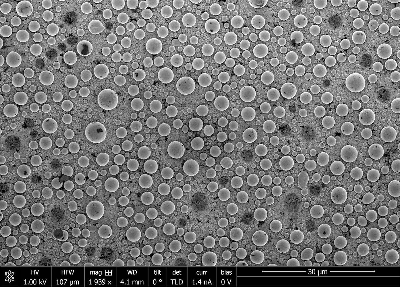
Scanning electron microscopy (SEM) is a surface imaging technique that achieves nanometer-scale resolution: orders of magnitude smaller than is possible with optical microscopy.
In addition to standard SEM detectors, all Covalent instruments are also outfitted with energy dispersive spectroscopy (EDS) detectors to capture quantitative elemental composition measurements, as well as 2D elemental maps, alongside conventional SEM images.
Strengths
- Top-down or cross-section imaging with nm- resolution
- Sub-nm resolution possible; see ‘high resolution’ technique variant
- Multimodal morphology characterization of surface or subsurface features
Limitations
- Specimen damage can occur during imaging