Are You Using the Right Detector?
4 Things to Remember for SEM
What are the different types of detectors?
SEM collects data using detectors that are stationed within the instrument. These detectors can be mounted within the sample chamber, at the electron emission anulus, or alongside the electrical lenses. The types of detectors vary from instrument to instrument. Each type of detector can have different ideal conditions (high or low vacuum, high or low keV, fast or slow scan speed) and can receive different signal types. Some detectors specialize in secondary electron (SE) signals, while others focus on collecting backscattered electrons (BSE). To better understand the detectors that are available, click here, we have created a handy reference chart. Understanding the detectors that are available and how the choice of detectors and instrument settings affects data can help refine the measurements as well as create a complete image of the sample.
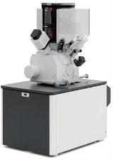
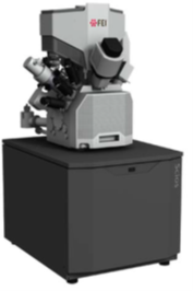
Figure 1: Both the Helios 5 UC DualBeam and Scios DualBeam contain multiple detectors to optimize critical signal gathering
Where is your contrast coming from?
Contrast results from the scattering efficiency of a signal type and allows for a clear understanding of a sample. In measurements with insufficient contrast, sample features (or defects) can be lost, and a sample’s characterization may be incomplete. Contrast results from SE and BSE differently, requiring researchers to understand the desired results for the best contrast refinement. SEs are particularly surface sensitive, and are often preferentially produced at surface features such as bumps or ridges, cracks, facets, or fine texturing. As a result, areas with distinguishable surface characteristics appear lighter in the image. For BSE, materials with higher atomic numbers create more scattering interactions, resulting in lighter areas in the scan. Likewise, darker scan areas indicate weaker scattering from lighter materials.
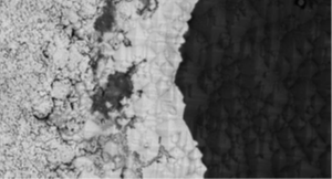
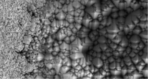
Figure 2: A single sample, captured with different amounts of contrast from separate detectors. From Covalent Metrology’s Covalent Academy webinar #18, “Expert Lessons on Electron and Ion Beam Imaging and Interpretation”
Is your accelerating voltage penetrating below the surface?
The power of the primary electron beam can be varied and can change the necessary equipment used to optimize the measurement of a sample. Typical voltages range from 1keV to 30keV, depending on sample sensitivity, vacuum requirements, and desired results. Higher accelerating voltages allow for greater penetration into the sample and increased visual depth. These voltages are often easier for new users, with better resolution and fewer effects from surface aberrations but may not provide a complete picture of the sample. As the main beam drops in voltage, small details on the surface become more enhanced, allowing for a better understanding of surface appearance and composition. Although increasing detail, lower beam voltages decrease both resolution and ease of use, introducing possible complications. The choice of accelerating voltage is usually dependent on what information about the sample is desired. For example, choose high accelerating voltages if you focus on material contrast, and choose low accelerating voltages if you desire surface details. Multiple accelerating voltages are often used to establish a complete understanding of the sample.
Figure 3: SE images of Tantalum hand on a barium/carbon/oxygen oval on a cracked iron/tantalum/silicon substrate taken with different accelerating voltages. From Covalent Metrology’s Covalent Academy webinar #18.
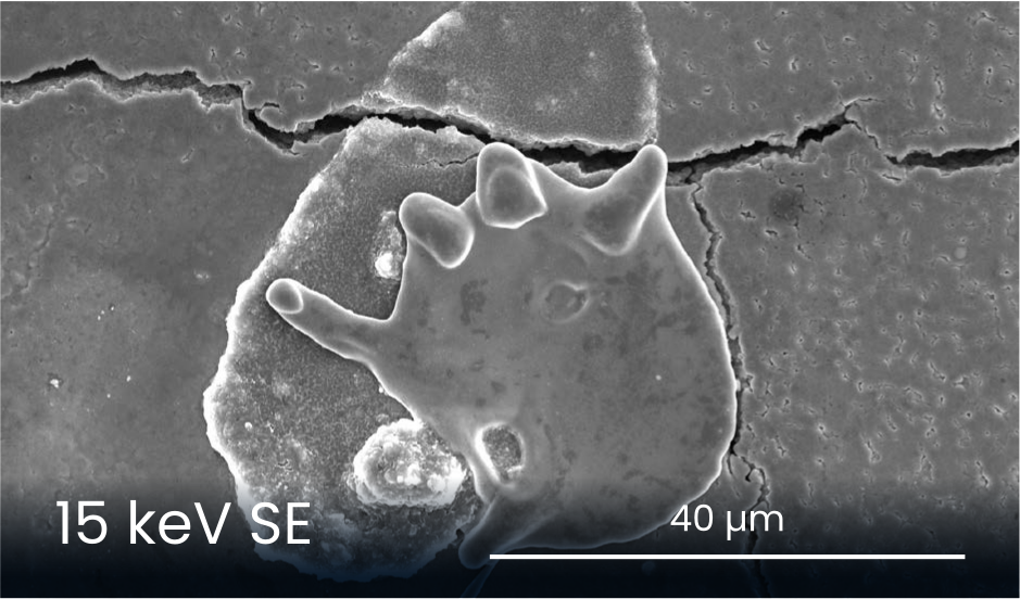
Higher accelerating voltages provide better resolution and electrons are less affected by aberrations. May be easier for new users, but surface detail may be obscured.
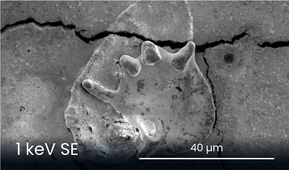
Lower accelerating voltages provide better surface detail but electrons are more vulnerable to aberrations. Below 2 keV may challenge inexperienced users and ultimate resolution is diminished at very low keV.
Figure 4: BSE images of Tantalum hand on a barium/carbon/oxygen oval on a cracked iron/tantalum/silicon substrate taken with different accelerating voltages. From Covalent Metrology’s Covalent Academy webinar #18.
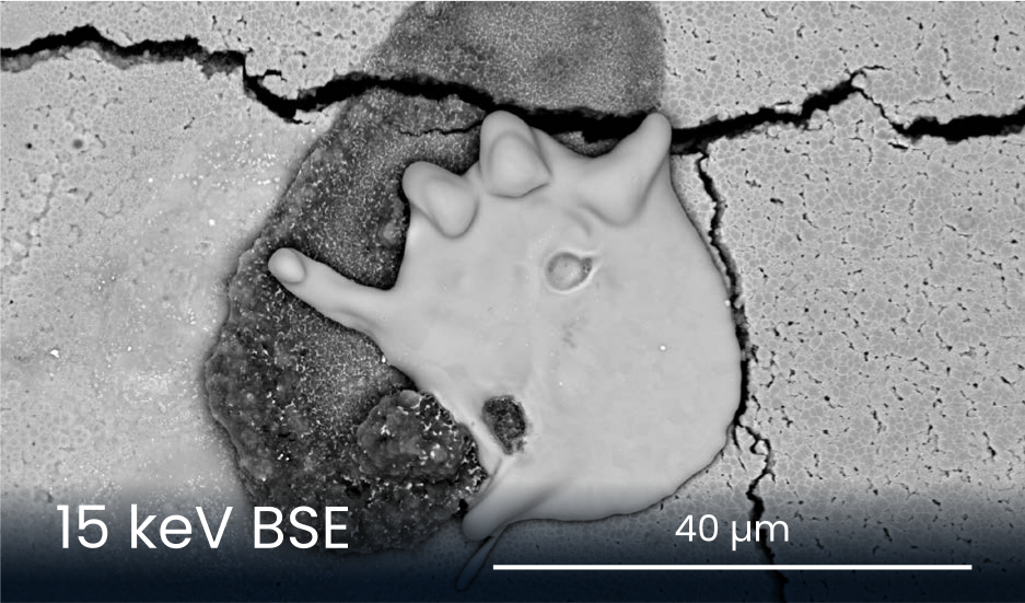
Higher accelerating voltages provide better resolution and electrons are less affected by aberrations. May be easier for new users, but surface detail may be obscured.
Higher resolution, with excellent materials contrast. Image can reliably be interpreted as: dark = low atomic number, bright = high atomic number.
What angle is your detector at?
Detector locations depend on their types and requirements. Some detectors are located inside the instrument’s column, while others are situated at lower angles around the chamber. A detector’s position affects the signal it picks up and can be refined with instrument modifications. When electrons are scattered from the sample, the angle of the scattering is influenced by the primary beam’s energy, the sample itself, and any electric biasing of the sample stage. BSE collected at high angles (closer to the primary beam) tends to be less dependent on the sample surface and more indicative of compositional information. Low angle BSE (collected closer to sample) are more sensitive to the sample’s topography and will carry topographical details. SE detectors, such as the standard Everhart-Thornley detector (ETD), are often placed at an angle to improve the detection efficiency of the SEs. This placement also allows for electric biases and increased attraction and detection of the secondary electrons.
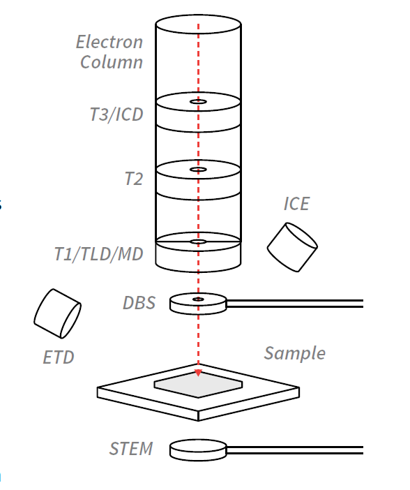
In-Chamber Detectors
ETD (generic) = Everhart-Thornley detector
- Found on all “full sized” SEMs, on 90% of the systems
- SE with positive grid bias,
- High-angle BSE with negative bias
DBS (Thermo Scientific) = Directional Backscatter detector (9 segments)
- Very sensitive at low keV and low beam current
- Fast scan speeds
- Each segment is individually addressable (can combine/subtract other segments)
ICE (Thermo Scientific) = In-Chamber detector
- Similar to the ETD (higher sensitivity, higher grid bias range)
- Electron and ion imaging
In-Column Detectors
ICD = In-Column detector
- In-column BSE detector
- When used with stage bias, also collects SE
- Solid state detector
TLD = Through Lens Detector
- Works in SE or BSE mode with varying suction tube biases
- Designed for UHR image with immersion lensing
- May be used for deep hole imaging with maximized suction tube voltage
MD = Mirror detector
- Single segment backscatter detector
- Works in immersion and non-immersion mode
- Works with beam deceleration/stage bias
Helios 5 UC DualBeam
T3 = Trinity 3
- Insertable in-column detector, sensitive to SE
- Highest resolution, lowest signal detector
T2 = Trinity 2
- Found on all “full sized” SEMs, on 90% of the systems
- SE with positive grid bias,
- High-angle BSE with negative bias
T1 = Trinity 1
- In-lens BSE detector, allows BSE imaging at tilt
- May be used in high or low vac modes
LVD = Low Vacuum Detector
- SE detector
- Designed for low vacuum mode imaging
Scios DualBeam
SEM analysis with Covalent Live View
Covalent Live View makes data collection more immersive.
Wherever you are in the world – you can now participate in your sample’s live analysis session with a Covalent Expert. You’ll see what our experts see through Covalent Live View. Experience cutting-edge instrumentation first-hand and discuss your analytical project in real-time as it unfolds.
Live View with Covalent Experts to:
- Deepen your understanding of the analysis with full context
- Ensure the critical information targets are gathered with imaging or EDS
- Collaborate with the measurement expert to optimize your metrology project in real time
- Invite your colleagues to combine measurements, analysis, and pathfinding simultaneously!
The Live View service is available with SEM analysis free of charge!
Learn more about Covalent Live View
SEM Analysis at Covalent Methodology
Covalent Metrology’s SEM Analysis team is led by Dr. Avery Green, who has worked extensively with advanced Scanning Electron Microscopy (SEM) and Focused Ion Beam (FIB) analysis. Dr. Green and his team utilize the cutting-edge instrumentation from Thermo Scientific to deliver high-quality SEM data with rapid turnaround times.
Our Helios 5 DualBeam provides excellent resolution for enhanced measurement and visualization – with specialized features particularly beneficial to clients characterizing devices or complex nanostructures. Our Scios DualBeam has comparable ultra-high resolution with immense adaptability to accommodate challenging materials: including samples previously untenable on an electron microscope.