
Multilayer Thin Film Characterization
Composition, thickness, uniformity, performance
Understand Multilayer Thin Films on a New Level
Multilayer thin film devices are a cornerstone of modern photonics enabling precise light manipulation across many applications like laser optics, displays, and telecommunications. High performance devices and innovation in this field require high quality films controlled thanks to characterization of key properties such as smoothness, uniformity and optical performance.
Covalent’s Silicon Valley lab is equipped to offer comprehensive characterization of multilayer thin film stacks.
- Elemental composition of the films making up the stack
- Composition gradients
- Thickness of each layer of the stack
- Refractive index of each layer of the stack
- Mapping of composition, thickness, optical properties across 300mm
- Surface roughness measurement
- Roughness of interfaces between layers
- Detection of contaminants down to ppms, ppbs
- Detection of voids and delamination
- Scratch test, adhesion test
- Mapping and High Resolution Electron Microscopy imaging with EDS elemental analysis
Advanced Modeling
Covalent provides advanced optical modeling solutions that empower teams to optimize new designs by accurately predicting how changes in layer composition and thickness will impact optical performance.
Common Thin Film Applications
Antireflective (AR) and High-Reflectivity (HR) Coatings
Bandpass Filters
- Telecommunications
- Fluorescence microscopy
- Spectroscopy
Dichroic Filters
- Projection systems, cameras, lighting
Sensors
Laser Optics
- Telecommunications
- Fluorescence microscopy
- Spectroscopy
Waveguides and Integrated Photonics
- Photonic integrated circuits (PICs), such as modulators and wavelength multiplexers/demultiplexers
Display Technology
- Liquid crystal displays (LCDs)
- Organic light-emitting diodes (OLEDs)
- Augmented reality (AR)
Analysis Example: Multilayer Anti-reflection
Coating for Camera Lens
Challenge
Determine structure, optical properties, and anti-reflection (AR) performance without any starting knowledge of an AR coating
Approach
Cross Sectional EDS
Material identification, layer configuration, and approximate thicknesses.
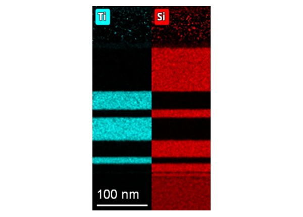
EDS maps of stack cross-section used to determine composition and thickness of stack layers.
Spectroscopic Ellipsometry
Optical model development, precise layer thickness measurement, measurement of optical property spectra for each layer.
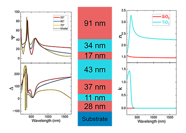
Spectroscopic ellipsometry combined with advanced optical modeling yield stack layers thicknesses, composition and optical properties (n,k).
Optical Device Simulation
Simulation of AR coating performance, and design optimization.
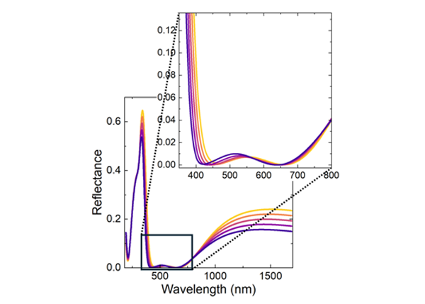
Advanced modeling also allows to simulate variations in stack design and guide efforts to optimize device performance.
Results
Starting with zero knowledge of the coating and substrate, cross sectional EDS combined with spectroscopic ellipsometry produced data that Covalent experts used to create an accurate optical model of the device. Advanced simulation was then successfully used to recommend changes in design to achieve a better performing AR coating.