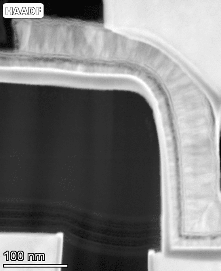
Transmission Electron Microscopy (TEM)

Transmission Electron Microscopy Main Image
This TEM micrograph shows the same interface as above, captured at 410kx magnification. At this level of magnification, it is possible to see individual columns of atoms in within the crystalline domains of the materials.

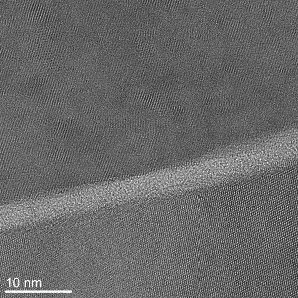
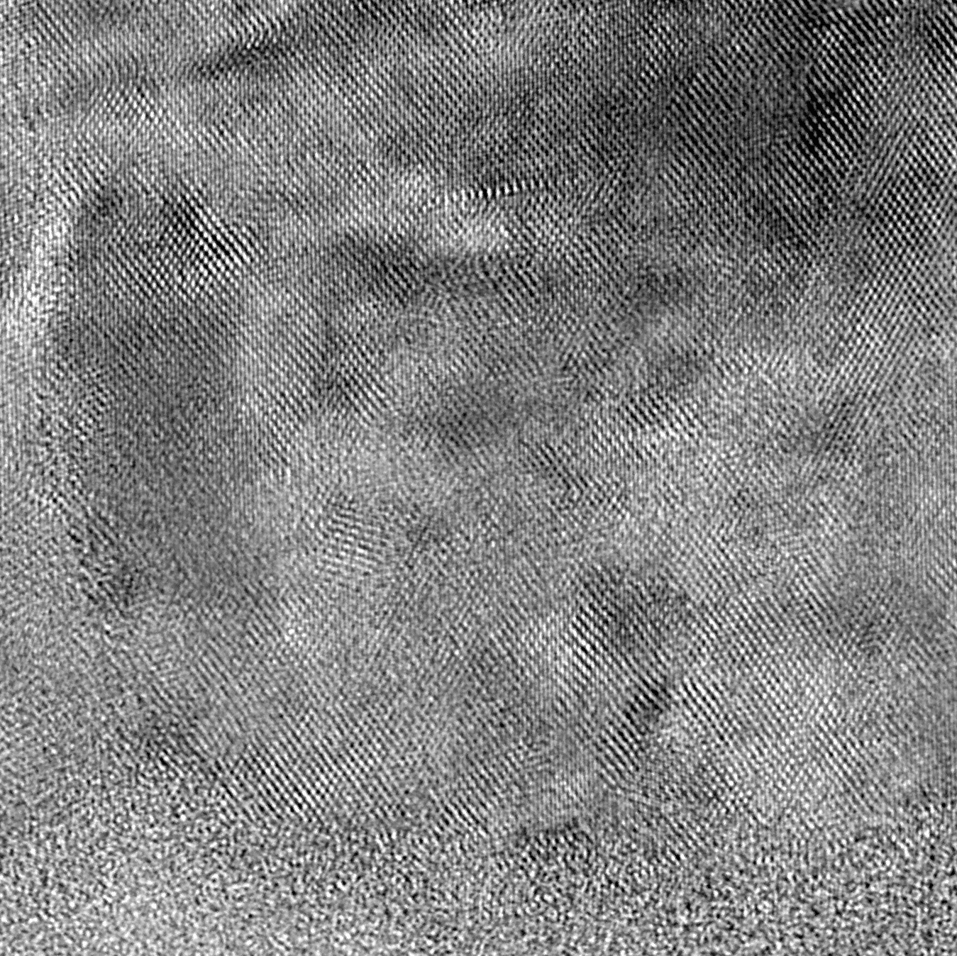
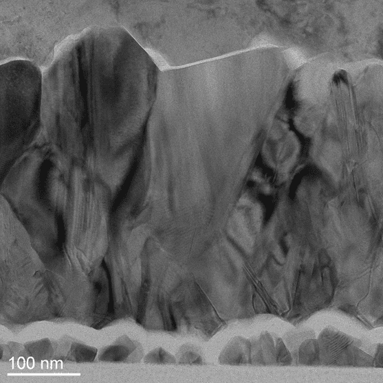
Transmission electron microscopy (TEM) is the highest-resolution imaging technique available today. It is used to visualize sample features with atomic-level spatial resolution limits to characterize the morphology of complex nanostructures.

“These are incredible images. Thanks for the preview.
It is so satisfying to get definitive answers to our questions!”
Brad Aitchison, Sr. Process Engineer, Redlen Technologies

Strengths

  • Highest possible spatial resolution: limit is atomic-scale
  • Bright Field and Dark Field imaging
  • Distinct imaging modes allow isolation of certain types of contrast information
  • Compatible with chemical (EDS) analysis and electrochemical analysis (EELS) techniques
  • Tomography and 3D reconstruction

Limitations

  • Requires extensive sample prep (normally performed with a FIB-SEM)
  • Specimens can be damaged if low dose techniques are not employed
  • Minimal topographical sensitivity
  • Typically only able to image a very small portion of the sample

Learn More

Sample Requirements

TEM Example Outputs

Ultra high resolution brightfield TEM image captured with the 4k Gatan OneView camera.

HAADF (High-Angle  Annular Dark Field) STEM image of a MiM (Metal – Insulator – Metal) capacitor structure within an integrated circuit.

TEM micrograph capturing the interface between two layers of distinct materials with various crystalline phases. This image was shot at low mag (35kx magnification).

This TEM micrograph shows the same interface as above, captured at 410kx magnification. At this level of magnification, it is possible to see individual columns of atoms in within the crystalline domains of the materials.

TEM Instruments Used

JEOL JEM-F200 Microscope

JEOL JEM-F200 Microscope

  • Cold-Field-Emission Gun (CFEG) Electron Source
    • Accelerating Voltage: 80 kV or 200 kV
    • High current and beam stability = ultra-high spatial resolution
    • TEM Point Resolution: 0.19 nm
    • STEM-HAADF Resolution: 0.14 nm
  • High Energy Resolution: 0.3 eV
  • High-res Electron Energy Loss Spectroscopy (EELS)
    • Fine Structure/Oxidation State Determination
    • Plasmon Resonance Analysis (CFEG supports zero-loss peak)
  • Gatan GIF Continuum ER Image Filter for Energy Filtered TEM (EFTEM) for light-element materials
  • Dual SDD Energy Dispersive X-ray Spectroscopy (EDX/EDS) detectors
View Instrument Brochure
ThermoFisher Scientific  Talos F200X (S)TEM

ThermoFisher Scientific Talos F200X (S)TEM

  • TEM Line Resolution: ≤ 0.10 nm
  • TEM Information Limit: ≤ 0.12 nm
  • Maximum Alpha Tilt: ± 90°
    (with tomography holder)
  • Maximum Diffraction Angle: 24°
  • Electron Source: High-Brightness Field Emission Gun
  • Gatan OneView CCD: 16MP 4K camera
  • Quad-EDS Detectors for enhanced sensitivity and detection limits
View Instrument Brochure

In a TEM, a high-energy electron beam is applied to a very-thin sample (a lamella), which is prepared to be electron-transmissive i.e. typically 20 to 50 nm thick.

As the beam passes through the sample, scattering interactions occur between its electrons and the atoms present which alter the transmitted beam intensity. These scattering events can produce several types of contrast in the final image, including: amplitude contrast (arising from atomic number and mass/thickness) phase contrast (from quantum phase shifting due to multiple scattered beams’ interference), diffraction contrast (from crystal structure and orientation), and more.

Different imaging modes on the TEM can target certain types of contrast over others, facilitating specialized analysis of relevant information.

The electron beams transmitted through the sample are focused by the TEM objective lens to form an image below it. This image is then magnified through a final series of electromagnetic optics, and detected by a specialized CCD camera.

Learn more about using Transmission Electron Microscopy services today!