What is Scanning Electron Microscopy (SEM)?
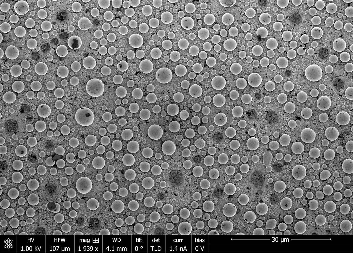
A Scanning Electron Microscope (SEM) scans the surface of solid samples living and nonliving by rastering a high-energy electron beam. Because of the high accelerating voltage used to power the electron beam, SEMs yield resolution limits orders-of-magnitude improved over conventional light-based microscopes.
Why Use SEM Analysis?
- High-resolution imaging gives exceptionally detailed scans of surfaces and buried features at the sub-micron level
- Probes surface texture and topography and enables critical dimensional measurements necessary for optimizing processes and quality control
- Streamlines material characterization: combining structure/morphology, and elemental composition insights
- Facilitates characterization and dimensional measurements of particles and aggregates
- Offers a variety of imaging modes–from backscattered electron imaging and secondary electron imaging to cathodoluminescence for multifaceted analysis
- Combining SEM with a Focused-Ion-Beam (FIB) enables cross-sectional analysis of subsurface structures and interfaces, particularly useful for investigating coatings, multilayer stacks, and nanoelectronic structures relevant to semiconductor devices
- Enables the most accurate single-particle sizing for industries that rely on precise particle proportions, such as environmental and pharmaceutical science.
SEM analysis significantly reduces the need for excessive preparation and processing times. As a result, SEM can quickly provide valuable materials insights involved in manufacturing quality control, forensic investigations, and other fields demanding time-sensitive decisions.
Applications of SEM
Materials Science
SEM magnifies the finest surface features of material samples, enabling analysis of nanoscale structures smaller than optical wavelengths. This is particularly useful when examining nanoscale defects invisible to the naked eye, including craters, fissures, or delaminations. Industries benefiting from SEM include:
- Energy Storage and Energy Conversion
- Biotechnology & Medical Devices
- Pharmaceuticals
- Surface Engineering
- Nanotechnology
- Advanced Materials / Metals / Composites
Semiconductors and Electronics
SEM is invaluable to the semiconductor and electronics industries. It is intrinsic to failure analysis, and to efforts to optimize product performance and manufacturing processes. SEM further supports R&D in semiconductors and electronics by providing essential information about new materials, fabrication methods, and structure-property relationships.
How Does SEM Work?
In scanning electron microscopy analysis, high-energy electrons are directed in a focused beam at a solid sample, resulting in subatomic interactions that emit different signal particles used to analyze the material.
Backscattered and secondary electrons are used to create visual maps of the surface, enabling measurement and analysis of exposed features. X-rays provide additional information about the elemental make-up of the material, and are positionally mapped to specific regions of the surface.
SEM vs. STEM
Scanning Electron Microscopy vs. (Scanning) Transmission Electron Microscopy
Both scanning electron microscopes and scanning transmission electron microscopes involve a highly-focused, high-energy electron beam rastering over a sample; the two techniques differ in what signals are collected.
In SEMs, the instrument picks up only secondary and back-scattered electrons that are reflected from the sample surface, and produces an image based on the intensity of that reflected beam.
On the other hand, in STEM imaging, the specimens are actually so thin that the probe/primary electron beam is actually able to pass through the sample. These electrons transmit through the sample comprise the detected signal used to produce the STEM micrograph. Because STEM uses a higher accelerating voltage to drive electrons fully through the sample, it has an enhanced resolution limit (approximately 0.1 nm; as compared with the 1-5 nm limit for SEM).
Scanning electron microscopy (SEM) analysis is widely used in life and material sciences, as well as for failure analysis concerning compositional and morphological defects. Alternatively, STEM is the industry standard for nanomaterials and nanoscale device research, supplying the atomic-scale resolution required for evaluating crystal structures and identifying crystalline defects.
Why Choose Covalent Metrology for SEM Analysis?
Our clients trust Covalent Metrology for SEM analysis results that exceed their expectations. We provide industry-leading, high-resolution scanning electron microscopy capabilities that offer superior data essential for understanding and optimizing the quality of your materials.
- Enhanced R&D Capabilities: Our SEM analysis provides critical insights that can accelerate your research and development processes.
- Quality Control Improvement: High-resolution imaging helps identify and resolve material issues, potentially leading to improved product quality.
- Rapid Turnaround: For time-sensitive projects, Covalent offers expedited processing to deliver your data in as little as 24 hours.
- Comprehensive Reporting: We provide detailed analysis and full documentation of measurement conditions and results, offering you actionable insights.
- Support for Informed Decision-Making: Our data and analysis can help guide strategic decisions in product development and manufacturing processes.
Contact Covalent Metrology today to learn how SEM analysis will enhance your company’s reputation and success.