Stereoscopic Scanning Electron Microscopy (SSEM): A Breakthrough Alternative for High-Res Surface Profilometry
In this live webinar, Dr. Naohiko Kawasaki from Toray Research Center in Japan will share insights on investigating the chemical and physical properties of heterojunction interfaces using cutting-edge analytical techniques. As semiconductor devices keep shrinking in size, the intricate bonding interfaces within sophisticated packaging like 3D stacks and RDL (redistribution layer) interposers become critically important. This seminar will be useful for semiconductor packaging engineers, failure analysis experts, materials scientists, and R&D engineers who want to develop new techniques to characterize interfaces on a nanoscale within smaller and smaller electronic components. We look forward to seeing you in this enlightening session!
What You’ll Learn
- How high spatial resolution AFM-IR and STEM-EELS chemical structure analysis tools can be used for precise interface characterization.
- The value of in-situ TEM measurement of electrical properties for the study of contact resistance in scaled devices.
- Chemical analysis of the bonding interfaces as well as the layer-stack are explained through real-world case studies.
Access the On-Demand Recording
Whoops! This event has already taken place.
You can access the on-demand recording of the webinar in our Covalent Academy Learning Center here:
About the Speakers

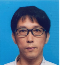
Dr. Naohiko Kawasaki
Manager of Electron Microscopic Analysis Team, Toray Research Center, Inc.
Dr. Kawasaki’s experience of over twenty years in various nano-scale characterization techniques includes STEM-EELS, cathodoluminescence, and in-situ TEM. His background includes research positions at the University of Tokyo, Université Paris-Sud, and a Doctor of Science degree from Kyoto University.
