Covalent Offers Fast, High-res Surface Imaging for Full Wafers with CT300 System
The new, high-resolution profilometer at Covalent Metrology enables non-destructive, high-speed imaging analysis on larger and more intricate samples than ever before.
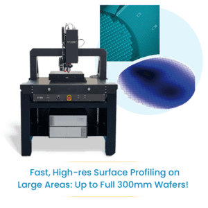
March 27, 2023 Sunnyvale, CA. Covalent Metrology, a premiere analytical services provider in North America, announced the installation of a high-speed profilometer from cyberTECHNOLOGIES, a leading manufacturer of advanced 3D surface measurement systems for industrial and scientific applications. The CT300 scans an order of magnitude faster than previous systems and accommodates a substantially enlarged scan area while maintaining nanoscale vertical precision. Ready now, the tool works best for non-contact imaging analysis on semiconductor wafers, PCBs, BGAs, micro-lens arrays, and microfluidic devices.
Optical profilometry is ubiquitous for measuring and mapping the subtle topographic features of flat surfaces. The CT300 is especially useful for inspecting wafers used to develop advanced nanomaterials and semiconductor devices. With a vertical resolution better than ~500 nanometers, the CT300 system can accurately measure surface roughness, map topographic variations, and quantify bow or warp across wafers up to 300 mm in diameter. These data empower engineers to refine the yield and quality of their fabrication processes.
Flexible optics in the CT300 preserve its high lateral resolution and broaden the range of its applications. In addition to wafers, more textured and 3-dimensional surfaces can also be characterized. Specialized detectors facilitate accurate depth measurements on and below the surface of transparent materials. The CT300 is a prime system for analyzing the hollow glass channels in microfluidic devices or measuring crucial parameters in finely-controlled optical materials, such as micro-lenses, light sensors, and components.
Beyond its flexibility and resolution, the CT300 is also unbelievably fast. It uses a linear sensor array to scan line-by-line (rather than the point-by-point raster used by past systems). This accelerates measurement speeds by an order of magnitude, enabling Covalent to offer faster turnaround times and more affordable imaging services on an expanded range of sample types.
“With the CT300, Covalent can continue to provide our clients with cutting-edge profilometry and topographical analysis capabilities,” said Dr. Avery Green, Director of Thin Film and Optical Metrology at Covalent Metrology. “It also marks an exciting expansion to our higher throughput solutions. Covalent can now offer differentiated services that help position us as a leader in surface analysis for semiconductors, optics, consumer electronics, medical devices, and beyond.”
Though this is the first cyberTECHNOLOGIES instrument to be installed at Covalent, the companies anticipate ongoing collaboration in expanding access to advanced analytical capabilities in North America.
“We are thrilled to be working with Covalent to expand awareness and develop new applications for the CT300,” said Karl-Heinz Strass, Managing Director at cyberTECHNOLOGIES. “The features of this tool could help engineers solve entrenched challenges in semiconductors, biotechnologies, medical devices, electronics, and more. Covalent is ideally positioned in the heart of Silicon Valley to help clients tackle those challenges with the CT300 profilometer.”
Learn More About Optical Profilometry Services
About Covalent
Covalent Metrology is a disruptive analytical services laboratory and digital platform based in Sunnyvale, California. Its mission is to empower technological innovation with superior data and insights. Covalent makes it easier and more affordable to access the metrology data necessary for strategic decision-making: facilitating faster research, development, and production of advanced materials and devices. It is dramatically changing the materials characterization service landscape with the combination of its modern data platform, world-class analysts and top-notch customer service, state-of-the-art analysis instrumentation, and strategic partnerships. Covalent now has over 500 customers in 30+ industries.  Learn more at: https://covalentmetrology.com
About cyberTECHNOLOGIES
cyberTECHNOLOGIES is a leading provider of high performance and easy-to-use high resolution 3D Optical Metrology Systems for non-destructive process control of Surface Topography, Roughness, Total Thickness, Flatness, Coplanarity, Pin Height & Position, Via Diameter & Depth, Film Thickness and Quality Inspection of Integrated Devices, Wafers, MEMS, Solar Cells, Fuel Cells, Lenses, Printed Products, Chip Packages, Ceramics, and many other related products.
For more information, contact:
Karl-Heinz Strass
Managing Director, cyberTECHNOLOGIES
khstrass@cybertechnologiesusa.com