Energy Dispersive X-ray Fluorescence (EDXRF), the core technique of the ONYX 3000 system, works by bombarding a sample with X-rays, which causes atoms in the material to emit secondary (fluorescent) X-rays. Each element emits X-rays at characteristic energies, so by measuring the energy and intensity of this emitted radiation, the system can identify and quantify the elements present in the sample. This is a non-destructive, surface-sensitive method ideal for analyzing thin films and multilayer stacks without damaging the wafer. The ONYX 3000 uses a micro-spot X-ray beam to provide localized analysis with high spatial resolution, essential for advanced node semiconductor manufacturing.
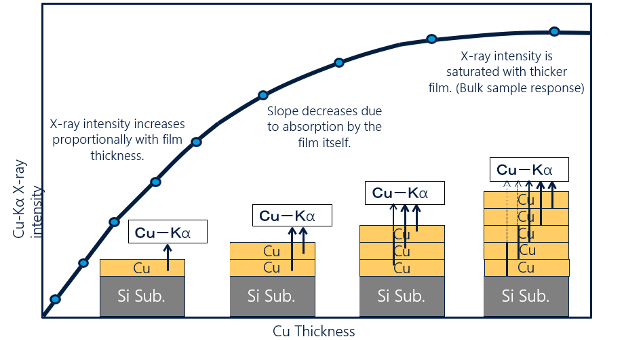
The mechanism of signal generation begins with an X-ray source exciting the atoms in the film. Detectors collect the emitted X-rays, and a spectrometer resolves their energies. The resulting spectrum is interpreted by sophisticated software algorithms, which deconvolute overlapping peaks and correct for matrix effects, such as absorption or enhancement due to neighboring elements or layers. By comparing the detected signal to known calibration standards, the system calculates material composition (atomic %) and thickness. When paired with optical techniques, the system also measures 3D topography.
The final output includes a detailed profile of the film or multilayer structure, including individual layer thicknesses, compositions, and uniformity maps. These insights enable engineers to monitor and control deposition processes, detect deviations from design targets, and optimize yield in real-time. In short, the technique provides a comprehensive picture of both the chemical and physical properties of thin films and wafer surfaces—essential for advanced semiconductor device fabrication.
Technical specifications:
Application range: Thickness and composition of thin films, nanometer (nm) to micron level (μm),
- Advanced Packaging: Solder bump composition: Ag%, Sn%, Ag/Sn ratio, Ni and Cu thickness, under bump metallization (UBM)
- FEOL/BEOL: metal films (e.g. Ga, Co, Ni, Ti, Pt), alloys (e.g. NiFe, CoNi, NiPt)
Incident optics for XRF: Polycapillary Mo x-ray tube (vertical incidence)
- Maximum rating: 50 W (50 kV / 1.0 mA)
- 17μm (@Cr Ka) typical (FWHM)
Receiving optics for XRF: Array of 4 FAST Silicon Drift detector (SDD) with 70mm2 active area
Sample stage: Vacuum chuck for ϕ300, 200, or 150 mm wafers
- Coupons, irregular samples, and smaller diameter wafers may be mounted on a carrier wafer for analysis
- X/Y stage resolution: < 1um, Accuracy: 0.1um
Pattern recognition: Bright Field capability
2D/3D Optical Technical specifications
Application range: Feature height and surface roughness
- Advanced Packaging: Solder bump height and CD
Optics: 2D microscope and 3D confocal microscope
3D Confocal Scanner Resolution: 100nm vertical / 1um lateral resolution
2D Microscope Resolution: 5 Megapixel Color CCD / 1um lateral resolution
2D Microscope Magnification:
- For 2x magnification: 5×5 mm FOV 2.7um pixel size
- For 10x magnification: 1×1 mm FOV 0.432 um pixel size
Sample stage: Vacuum chuck for ϕ300, 200, or 150 mm wafers
Measurements possible:
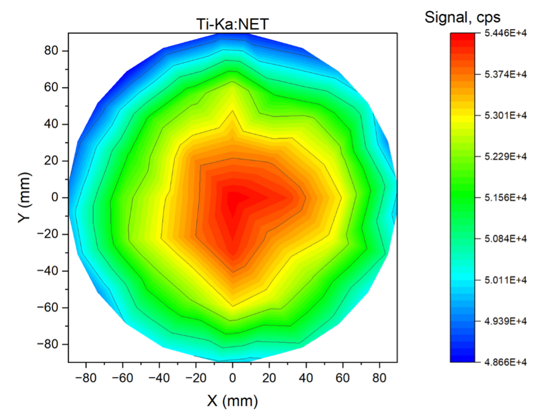
- EDXRF Spectrum Analysis: This spectrum displays the elemental composition of sediment samples, highlighting peaks corresponding to specific elements.
- Optical Microscopy Setup: Optical microscopy is employed for inspecting surface morphology and detecting defects in materials.
- Confocal Measurement Principle: A schematic representation of the confocal measurement technique, which enables high-resolution, three-dimensional imaging of surfaces, essential for assessing surface topography and roughness.