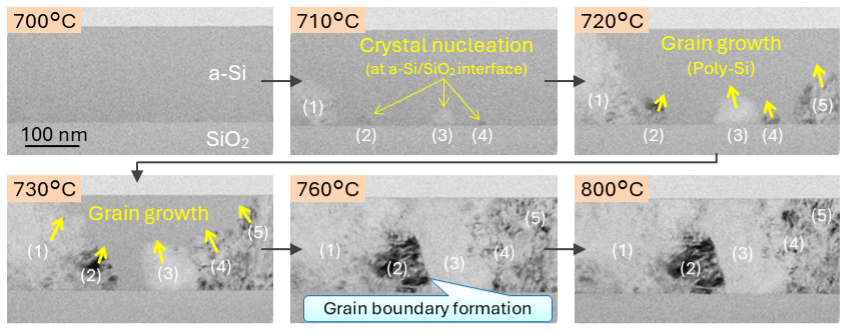
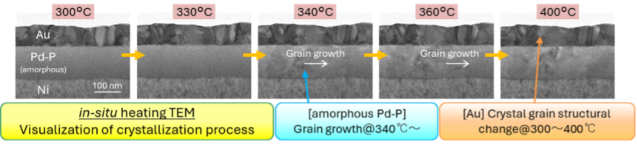
In-situ heating Transmission Electron Microscopy (In-situ heating TEM)

<em>In-situ</em> heating Transmission Electron Microscopy Main Image

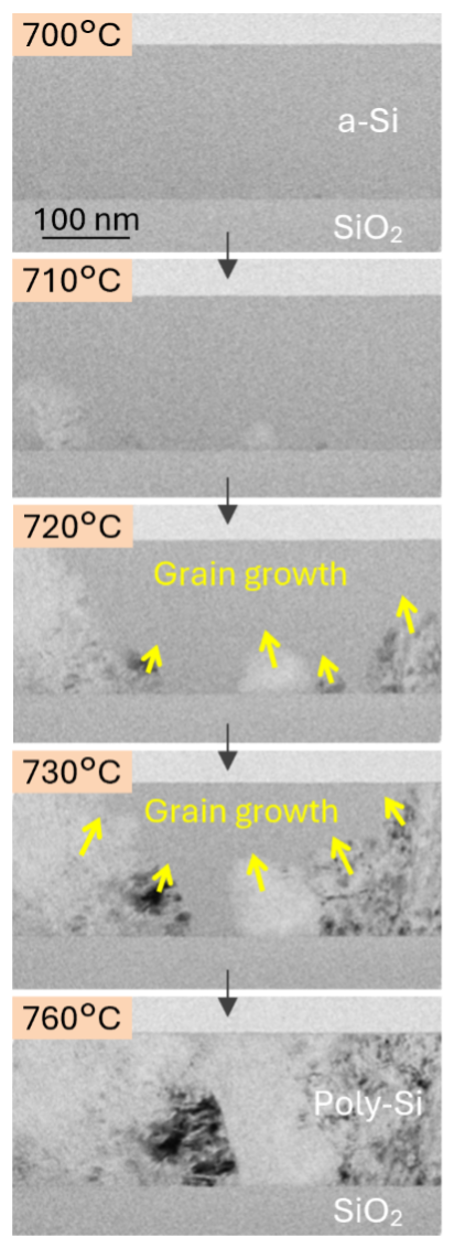
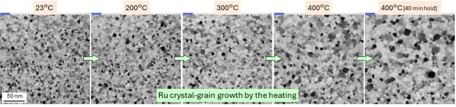
In-situ heating TEM technique make it possible to observe the thermal behavior of materials with nano-meter-level during heat treatment.

Semiconductors (including bonding interface), Metals, Nanomaterials, etc.

Strengths

  • Observation at multiple temperatures in a single sample
  • Visualization of thermal behavior at the same position: starting point of change (When? Where?), and Process of change (How?)
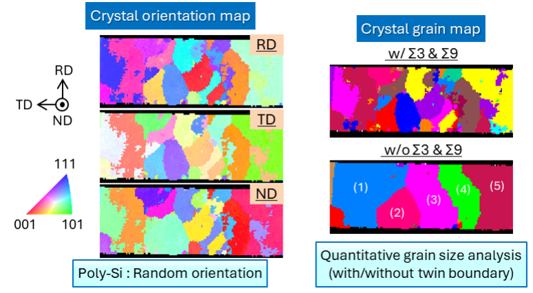
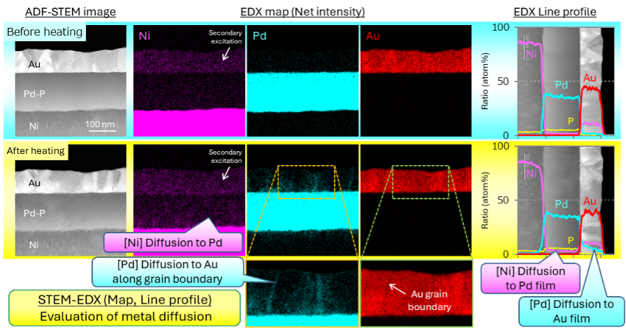
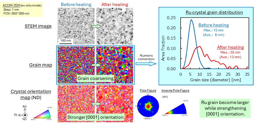
  • Combination with other (S)TEM-based methods from the same field of view as in-situ heating TEM:
    • Crystal orientation analysis, Grain size analysis: ACOM (Automated Crystal   Orientation Mapping)-TEM
    • Elemental composition analysis (elemental diffusion): EDX (Energy Dispersive X-ray spectroscopy) / EELS (Electron Energy Loss Spectroscopy)

Limitations

  • Atmosphere: in vacuum (not gas, not under pressure)
  • Evaluation sample: thin film (not bulk)
  • Effects of electron irradiation (e.g., reaction acceleration): it can be reduced by optimizing the electron beam irradiation conditions

Learn More

Sample Requirements

Specialized lamella prepared and mounted on Heating chip

*We provide sample preparation for in-situ heating TEM observation

In-situ heating TEM Example Outputs

Investigation of crystal-growth mechanisms using in-situ heating TEM and ACOM-TEM techniques

Sample: Amorphous silicon (a-Si) film

Cross-sectional TEM images of Si film during heating process

Crystal orientation map and Crystal grain map of crystallized Si film after heating process by ACOM-TEM

Cross-sectional TEM images of metal multilayer film during heating process

Thermal behavior of metal multilayer film investigated by in-situ heating TEM and STEM-EDX techniques

Sample: Metal multilayer film (Au / Amorphous Pd-P / Ni)

Plan-view in-situ heating TEM observation of Ru thin film

Evaluation of metal diffusion before and after heating process by STEM-EDX analysis


Plan-view in-situ heating TEM observation during crystal grain growth process of Ru thin film

Sample: Crystal ruthenium (Ru) thin film (Film thickness: 12 nm)

Plan-view in-situ heating TEM observation of Ru thin film

In-situ heating TEM Instruments Used

  DENSsolutions <em>In-situ</em> TEM holder

DENSsolutions In-situ TEM holder

  DENSsolutions Heating chip (Nano-Chip)

DENSsolutions Heating chip (Nano-Chip)

https://denssolutions.com/products/lightning/

How In-situ heating TEM Works

In-situ heating TEM system consists of a dedicated TEM holder, heating chip and external temperature control unit. There are several holes for TEM observation in the central part of the heating chip, and thin TEM specimens must be set on the holes. Using this system, specimen temperature can be controlled precisely in TEM equipment.

Possible measurements:

Direct observation of thermal behavior at nm level during heat treatment: crystallization, crystal grain growth, metal diffusion, etc.

Combination with other (S)TEM-based methods at the same field of view: ACOM-TEM, EDX, EELS

Technical specifications:

Temperature range: 23(RT) – 1300 deg C (Free temperature design)

Learn more about using In-situ heating Transmission Electron Microscopy services today!