Scanning Capacitance Microscopy (SCM)

Scanning Capacitance Microscopy Main Image

Precise sample preparation and SCM analysis technology enable the evaluation of carrier distribution in semiconductors.

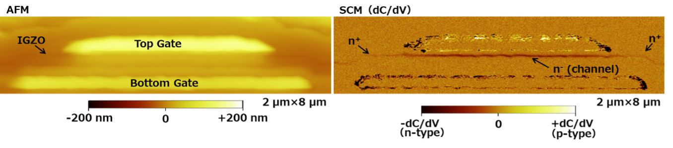
Application areas: semiconductors (Si, GaAs, InP, SiC, GaN, IGZO etc.)

Strengths

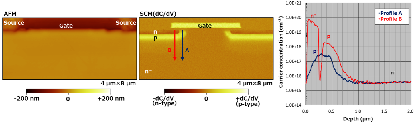
  • Evaluation of carrier distribution in localized areas.
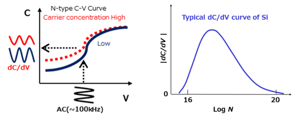
  • Wide measurement range from low concentration (just under 1E16 cm-3) to high concentration (about 1E20 cm-3)

Limitations

  • Measurement range is from just under 1E16 cm-3 to about 1E20 cm-3.
  • It is difficult to measure large steps or very thin layers of low concentration.
  • The spatial resolution depends on the carrier concentration: it is about 20 nm in high-concentration layers and about 100 nm in low-concentration layers.

Learn More

Sample Requirements

Semiconductor (Device and Wafer)

SCM Example Outputs

SCM observation of SiC-MOSFET and carrier concentration conversion (Semi-quantitative)

SCM observation of IGZO-TFT on flexible substrate: Channel length can be evaluated

SCM Instruments Used

Bruker Dimension XR (SCM option), NanoScope Ⅴ

Bruker Dimension XR (SCM option), NanoScope Ⅴ

How SCM Works

The change in capacitance when AC voltage is applied (the slope of the C-V curve, see picture on the top of the page) is detected by AFM’s conductive probe.

Note that the dC/dV signal increases as the carrier concentration decreases, but the dC/dV signal decreases below a certain concentration.

Technical specifications:

Measurements possible:

Learn more about using Scanning Capacitance Microscopy services today!