2.5D X-ray Inspection (2.5D X-ray)

2.5D X-ray Inspection Main Image
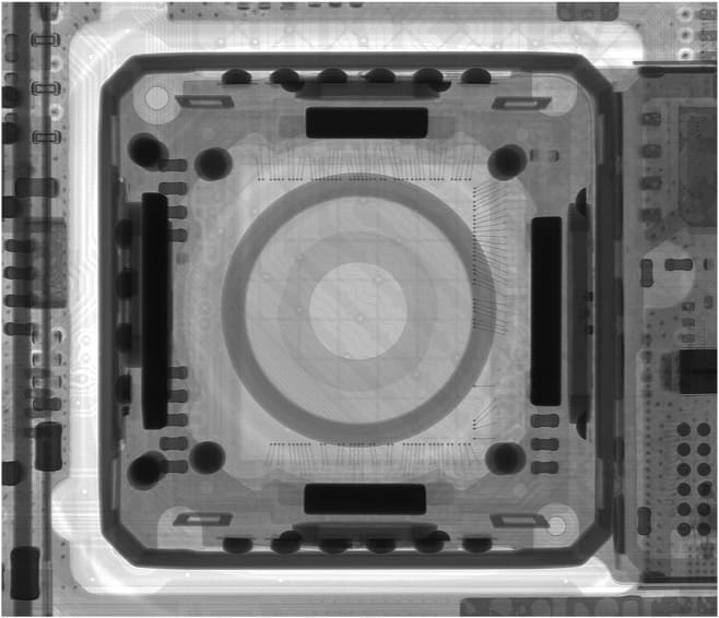
2D X-ray radiograph of the CPU chip in a modern cell phone.

2.5D X-ray inspection enables non-destructive imaging of the exterior and interior features of complex parts, assemblies, and devices from multiple angles. It is widely used for quality control on printed circuit boards (PCBs), machined components, medical devices, and more.

Strengths

  • Non-destructive
  • Characterization of obscured features
  • High throughput
  • Feature recognition down to 100nm
  • Automated inspection

Limitations

  • 2D projection only, no depth discrimination

Learn More

2.5D X-ray Inspection Services

2.5D X-ray Inspection

2.5D X-ray inspection enables non-destructive imaging of the exterior and interior features of complex parts, assemblies, and devices from multiple angles. It is widely used for quality control on printed circuit boards (PCBs), machined components, medical devices, and more.

Sample Requirements

Example Outputs

2D X-ray Radiograph captured on a conventional smart-phone. The X-rays illuminate interior features and components without requiring the deconstruction of the cellphone assembly.

Example 2.5D x-ray inspection of the internal componentry of the cell phone.

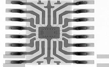
X-ray radiograph of a wire bonded component still in the package. Lead frame, bond wires, and die all clearly visible.

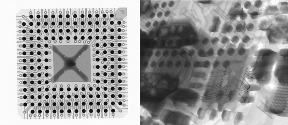
X-ray radiograph of an unbonded BGA board (left) and angled view of a wire bonded device and BGA soldered on opposite sides of a PCB (right). Cu traces, vias, solder balls, and solder voids clearly visible.

Instruments Used

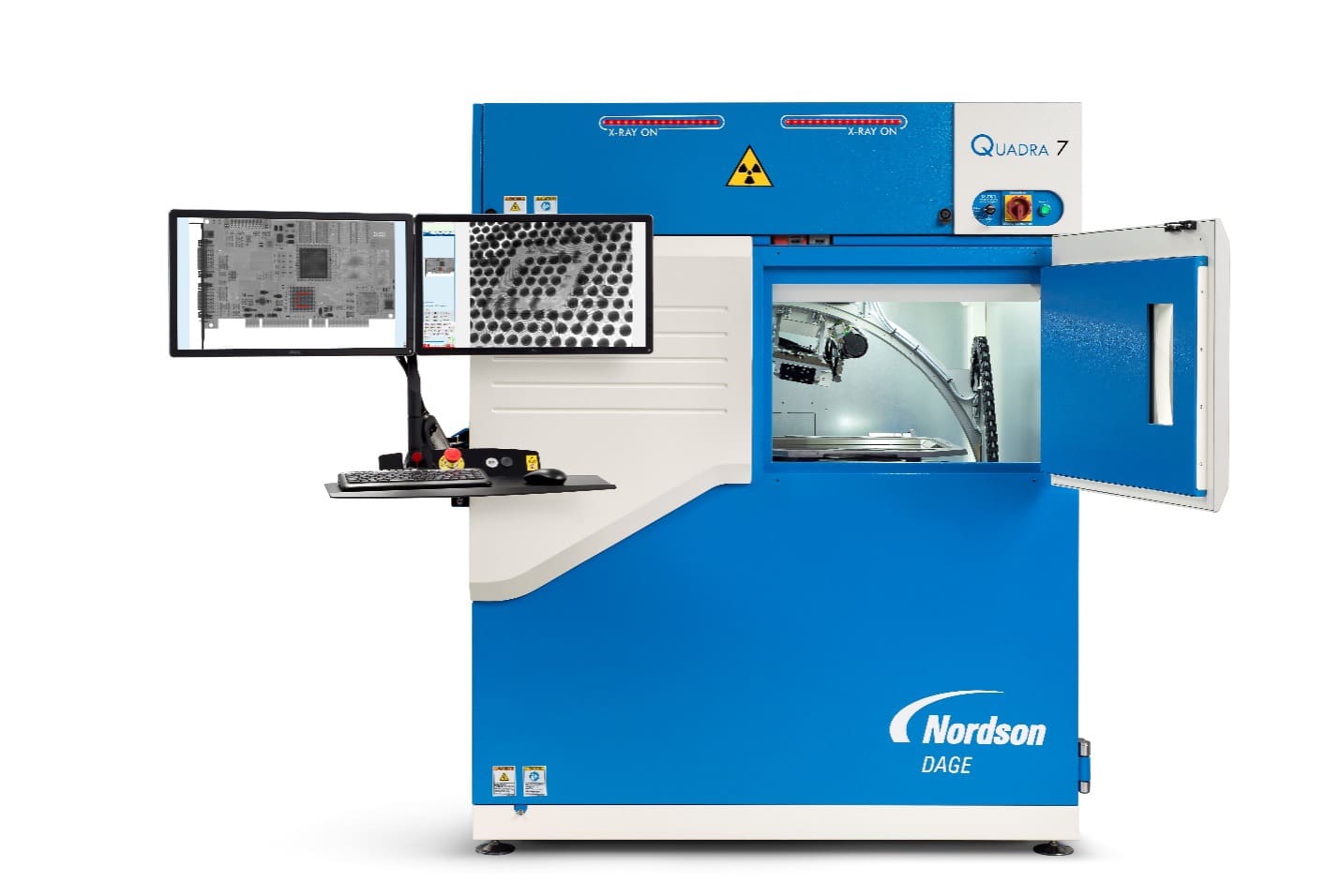
Nordson DAGE Quadra 7

Nordson DAGE Quadra 7

  • 30-160kV, 20W
  • 100nm feature recognition
  • 7MP flat panel digital detector
  • 30fps framerate
  • 0-70° oblique angle view
  • 20 x 17.5” inspection area
  • Geometric magnification up to 2.5kx & total magnification up to 68kx
  • High Dynamic Range (HDR) enhancement software
  • X-Plane CT scanning of BGA solder balls
  • Dosage control for X-ray sensitive samples
View Instrument Brochure

How 2.5D X-ray Works

X-ray inspection systems use a point source to emit high-energy X-rays which pass through your sample. The transmitted X-ray photons are projected onto a detector, resulting in an image whose contrast is determined by the densities and thicknesses of the sample materials. Denser and thicker materials absorb more X-rays and are subsequently represented as darker regions in the final image. A high-pixel density digital detector enables an operator to generate these images in real time. In conjunction with sophisticated analytical software, modern detectors have enhanced the accuracy, useability, and throughput of modern x-ray imaging systems.

The source voltage can be manipulated to alter the spectral range of the emitted X-rays. Higher energy X-rays have a lower attenuation coefficient, meaning more photons will pass through a given feature. By adjusting source voltage and other parameters, such as exposure time, the system can be fine-tuned to produce optimal images on a variety of samples.

X-ray inspection is frequently employed for failure analyses or quality control inspections on PCBAs, electrical components/ICs, BGA solder balls, welds, batteries, precision machined components, and surgical implants.