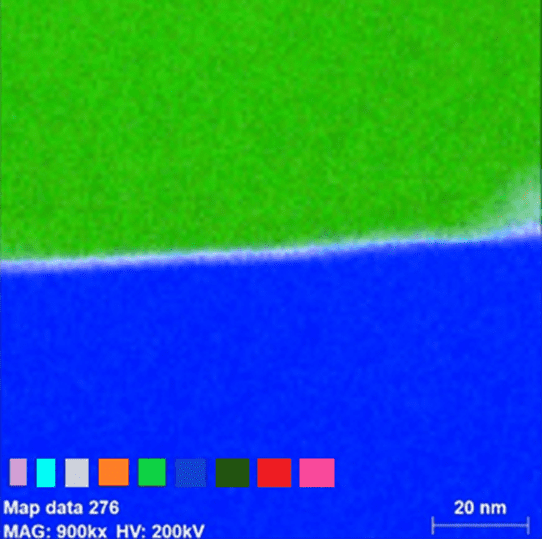
Scanning Transmission Electron Microscopy (STEM)
Scanning transmission electron microscopy (STEM) is a hybrid electron microscopy technique used for imaging and morphological characterization with atomic-scale resolution.
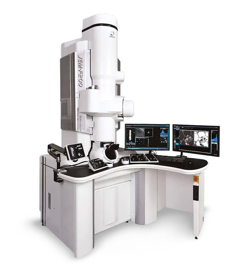
STEM is available on both Covalent’s FIB-SEM instruments, as well as our TEM. All Covalent (S)TEM systems have fully integrated energy-dispersive x-ray spectrometers (EDS or EDX) for correlative elemental composition and mapping analysis.
Strengths
- Atomic-level resolution limit – substantially improved over conventional SEM
- Enables spatial correlation of advanced TEM signals:
- Energy-dispersive X-ray Spectroscopy (EDS / EDX): elemental composition and mapping
- Electron Energy Loss Spectroscopy (EELS): bonding state and light element analysis with some electrochemical insights
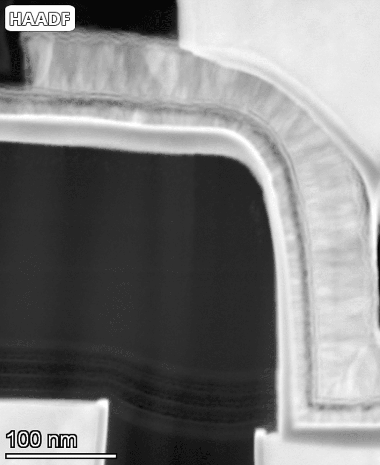
- High-Angle Annular BF, and DF scattered beams (HAABF / HAADF): standard ultra-high-resolution imaging with additional atomic-number contrast for mapping applications
- Kikuchi Bands: crystallographic analysis for electron diffraction patterns
Limitations
- Requires extensive sample preparation to generate a thin-enough analytical window for the material to be electron-transmissive
- High-energy, the highly-focused electron beam can cause sample damage